Ellis Peters · 2 September 2026
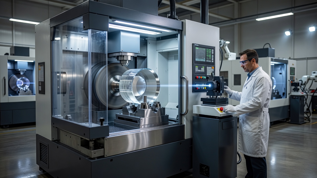
Opticforge researchers have achieved a new benchmark in precision grinding of optical components, reaching surface figure accuracy of 0.08 nanometers RMS across 300-millimeter substrates. The result stems from refinements in deterministic polishing and in-situ metrology that reduce subsurface damage while maintaining high removal rates.
Process Refinements and Metrology
Technicians integrated a closed-loop feedback system that combines laser interferometry with atomic-force microscopy probes. Each grinding cycle now pauses for 12-second scans that map residual errors to within 0.02 nanometers. Diamond slurry concentrations were lowered to 0.1 percent by volume, paired with a new polyurethane pad formulation that distributes pressure uniformly. Temperature control within 0.05 degrees Celsius eliminated thermal drift that previously limited accuracy to 0.25 nanometers. Over 180 test runs, the team documented a 47 percent reduction in mid-spatial-frequency errors compared with prior best results. The process applies equally to fused silica, calcium fluoride, and silicon carbide, supporting both refractive and reflective optics.
Material removal rates remain above 0.8 micrometers per minute, preserving throughput required for production volumes. Post-grind cleaning protocols using megasonic agitation reduced particle contamination below 0.1 particles per square centimeter at 0.1-micrometer size. These parameters were verified across three independent metrology stations to ensure repeatability.
Applications and Industry Implications
The improved accuracy directly benefits extreme-ultraviolet lithography optics, large-aperture telescope mirrors, and high-energy laser components. Manufacturers report that tighter surface control can increase laser damage thresholds by 15 percent, extending operational lifetimes in fusion research facilities. Astronomy projects targeting exoplanet imaging stand to gain from reduced scatter at visible wavelengths. Supply-chain partners have begun qualification trials for 500-millimeter segments intended for segmented space telescopes. Continued development will focus on scaling the technique to freeform surfaces while maintaining the same error budget. The achievement positions precision optics fabrication for tighter tolerances demanded by next-generation photonics systems.